


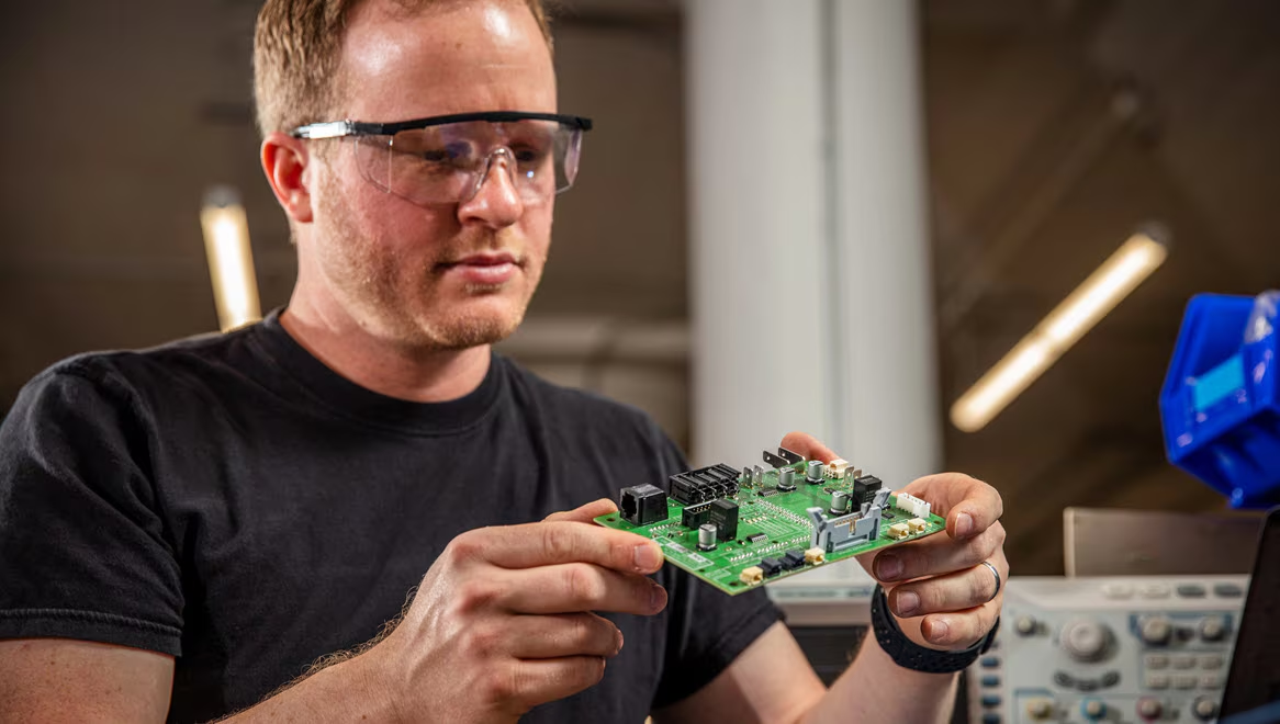
15+ years of solid experience – Multilayer, High complexity, Highly dense PCB Design Services. Experts in Reliable PCB Layout Design that results in Cost-Effective Products.

At Nevaloss Technologies, we deliver high-quality PCB designs tailored for performance, durability, and innovation. Our expertise spans from single-layer to multi-layer boards, ensuring precision layouts, compact form factors, and reliable connections. Below are a few examples of PCB projects that demonstrate our capability to support diverse industries, including IoT devices, automation systems, consumer electronics, and industrial hardware.
Professional customized PCB Design Services of all types, including, Multi-Layer, Rigid, Flex, Rigid-Flex
Highly Complex & Dense PCB layout designs done with speed & accuracy
Advanced component footprints & library creation including BGA, QFN packages as per IPC standards
High speed PCB design including differential pairs, length matching etc.
Expertise in critical & sensitive signal routing for Analog & Digital (Mixed Signal) circuits
PCB reverse engineering service
Re-engineering services to correct flaws or to optimize existing PCB designs for lowering costs
PCBA Prototyping
PCBA Manufacturing
Electrical & Functional Testing services of the designed PCB
Upgrade old PCBs with outdated & obsolete components to the latest technology with widely available SMT components
Do you already have a PCB done and need it to be professionally reviewed? Check out our PCB Design review services.
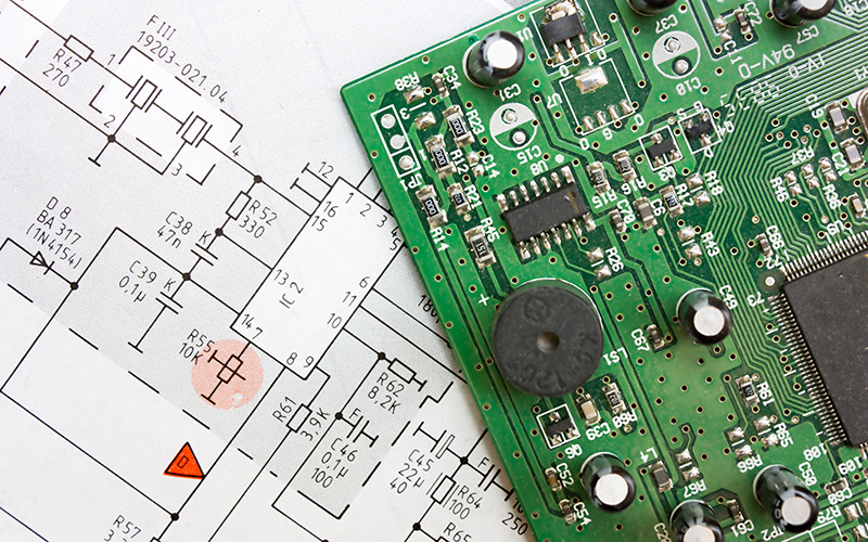
PCB is an acronym for Printed Circuit Board. A PCB layout is made to electrically connect the electronic components through conductive tracks and pads. It forms the backbone of all Electronic Design Services. Hence, it must be carried out with utmost care & responsibility. It can almost single-handedly determine the success of an Electronic Product. These components are soldered onto the PCB to provide electrical connectivity and to fasten them onto the board.

Single sided PCBs are the simplest form of circuit boards with components mounted on one side and conductive copper tracks on the other. They are cost-effective and ideal for low-density designs.

Double sided PCBs allow conductive copper layers on both sides of the board, enabling more complex circuit designs and better component density. They are widely used in power supplies, lighting, and automotive applications.

Multi-layer PCBs consist of three or more conductive layers stacked together. They offer high circuit density, improved performance, and are essential in advanced devices like smartphones, servers, and medical equipment.

Rigid PCBs are made from solid substrate materials that provide strength and stability. They are highly durable, easy to maintain, and commonly used in computers, industrial machines, and military equipment.

Flexible PCBs are made from flexible materials, allowing the board to bend and fold. They are lightweight, space-saving, and used in wearable devices, cameras, and medical instruments.

Rigid-Flex PCBs combine the durability of rigid boards with the adaptability of flexible circuits. They reduce space and weight, making them ideal for aerospace, automotive, and portable electronic products.
A PCB can also be designed according to your technological needs thus being the best possible fit to assemble your circuit. PCB design services start with a PCB designer who gathers all the product specifications and the requirements for your circuitry. Then using strategic design techniques, we create a best-fit PCB which is designed to cater to your needs, ensuring it meets industry standards and remains competitive in the market. Here are some key steps we follow to design a PCB:
PCB (Printed Circuit Board) design is the process of creating the layout for electronic circuits. It ensures proper electrical connectivity, mechanical stability, and reliability of the final product. A well-designed PCB improves performance and reduces manufacturing costs.
We design single-sided, double-sided, multi-layer, rigid, flexible, and rigid-flex PCBs. Our expertise covers everything from simple consumer electronics boards to complex industrial and IoT hardware solutions.
Yes, our team handles complete PCB design including schematic capture, component placement, routing, and final layout. We also ensure designs comply with industry standards and are optimized for fabrication and assembly.
Yes, along with design, we offer PCB prototyping and testing services. This helps validate the design before mass production, ensuring performance, reliability, and durability of the circuit.
We use industry-leading software like Altium Designer, Eagle, and KiCad for PCB design. Our designs comply with IPC standards and are tailored to ensure manufacturability and cost-effectiveness.
We’re here to explore how we can collaborate, leveraging our expertise to fuel your product development. Let’s get started and propel your business forward!